
How it started
When I started working at arculus as an electronics hardware engineer, one of my very first tasks was to revise our triple motor inverter, one of the key parts of our Robot Control Unit (RCU®). This is the very heart of our electronics system and the interface to the “muscles” of the arculee, the three permanent magnet synchronous motors we use for driving and lifting loads. It was a hugely interesting but pretty challenging task, especially given that I only had previous experience with simpler power electronics – even the strongest components I had ever designed had roughly only 10% of the power of one of our inverters.
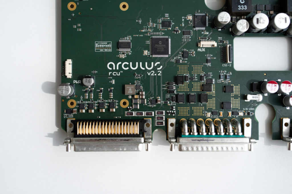
At this time, the concept of the RCU as a single Printed Circuit Board (PCB) system, including nearly all the non-safety-relevant functions of our robot, was already laid out, and arculus was fully committed to developing its own power electronics. We even had the first few samples designed and produced by an external contractor – the only problem being that they didn’t work. These inverters delivered only a fraction of the necessary power and regularly died without warning. Furthermore, the team had no real consensus on why this was the case. So the first step had to be a thorough investigation into inverter theory to identify the weak spots of the design at that point.
One of the first findings was that the Metal-Oxide-Semiconductor Field-Effect Transistor (MOSFETs) used so far in the power stages were not up to the job. Thus, we had to find a better-fitting replacement that could take the envisioned 40A from the 48V battery without overheating. One important feature is to reduce the amount of heat that is generated. For this, it is crucial to have both low resistance when the MOSFET is conducting, and swift, clean transitions between the switched-on and off states. Fortunately, after careful research, we could finally find enough parts to fulfil these requirements.
Keeping it cool
The other part of keeping the RCU® cool is transporting whatever heat is generated away from the chips – which turned out to be even more challenging. The first idea was to put the MOSFET’s plastic housing thermally into contact with our massive aluminium housing. But the plastic itself conducts the heat so poorly that even if the surface is cool, the chip inside can still massively overheat.
The thermal conductivity to the solder contact at the bottom of the chip is roughly 40 times better, but here our one-board construction containing both logic and power electronics posed yet another challenge. The high-speed interfaces and tight packaging in the logic part of the board demanded using only very thin 35µm copper layers in the board itself, as the small structures cannot be etched into thicker copper. But such a thin copper layer is not enough to conduct the heat of the MOSFETs away. Simply increasing the size of the Field-Effect Transistors (FETs) and thus increasing the contact area for more heat transfer was also not an option, as there was not enough space left. So I came to a dead end with the standard packages for MOSFETs.
Luckily, I then found the solution to the problem in the shape of the Infineon SuperCool MOSFET packages. These feature a cooling pad on top, which is thermally as well connected to the chip as the bottom pad used for the solder connections. By contacting these to our aluminium housing with thermally conducting material, I could remove the heat without routing it through the PCB, which is not built for the task. And I did not have to compromise on any electrical characteristics, as the chip itself is one of the OptiMOS 5 family that offers excellent performance parameters.
A long-living short story
In this way, I was able to pave the way for our custom inverters’ design, although many additional design tricks and cutting-edge parts were necessary to bring its performance to the point where it is today. Nonetheless, it was less than nine months from the moment I joined until the redesigned inverter ran tests at 100A – 2.5 times the current of its original design goal. That demonstrated an awesome team effort and showed that quality engineering does not have to take ages if the company structure allows it!